Applied Materials $5 Billion India Investment: Semiconductor Boost
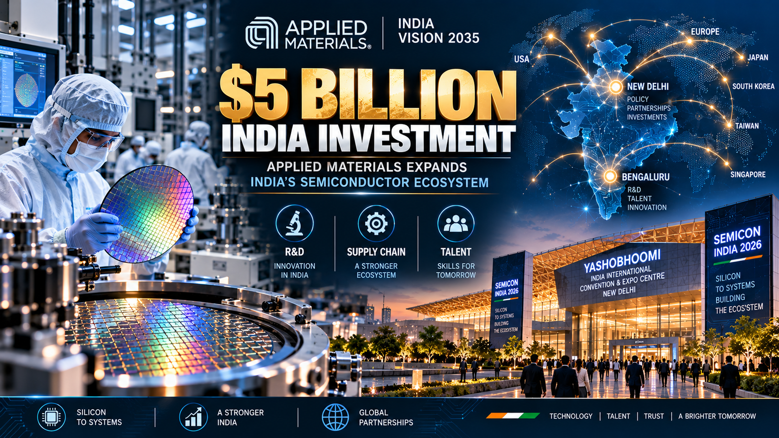
Applied Materials Announces $5 Billion India Investment: Major Boost to India’s Semiconductor Ecosystem
Date: 18 September 2026
Category: Science & Technology | Economy | Current Affairs
Exam Relevance: UPSC, SSC, Banking, State PSC, CDS, CAPF, Defence & Railway Exams
What Happened?
US-based semiconductor equipment company Applied Materials has announced a US$5 billion investment in India over the next decade under its “India Vision 2035” initiative.
The announcement was made during SEMICON India 2026, which is being held in New Delhi from September 17–19.
The investment is aimed at strengthening India’s semiconductor ecosystem through research and development, supply-chain expansion and talent development.
The Indian government has described the development as part of the country’s broader effort to build capabilities across the semiconductor value chain.
What Will the $5 Billion Investment Focus On?
Applied Materials has identified three broad areas:
1. Research & Development
The company plans to deepen its semiconductor R&D capabilities in India.
It has also announced plans for a 140-acre advanced semiconductor research park, designed to bring together cleanroom capabilities, engineering expertise and collaborative R&D involving customers and suppliers.
2. Semiconductor Supply Chain
Applied Materials aims to significantly expand India’s role in its global supply chain.
The company has announced an objective of increasing its India-based supply-chain capacity tenfold by 2035.
This could create opportunities for Indian suppliers and manufacturers participating in the semiconductor ecosystem.
3. Future Talent
The initiative also focuses on developing India’s semiconductor workforce.
The expansion is expected to strengthen opportunities for engineers, researchers and other professionals working in advanced semiconductor technologies.
Why Is This Important for India?
Semiconductors are no longer just an electronics-industry issue.
They are critical to:
- Artificial Intelligence
- Smartphones and computers
- 5G and 6G
- Electric vehicles
- Defence systems
- Satellites
- Data centres
- Industrial automation
- Autonomous systems
- Internet of Things (IoT)
The Indian government has therefore been attempting to build a complete semiconductor ecosystem rather than relying primarily on imported chips.
A major international investment in semiconductor equipment, R&D and supply chains can contribute to this wider ecosystem.
PIB notes that semiconductors are increasingly important for economic security, technological resilience and national self-reliance.
India’s Semiconductor Mission
India’s semiconductor strategy is being implemented through the India Semiconductor Mission (ISM) and the Semicon India Programme.
The first phase, Semicon 1.0, was designed to establish the foundations of semiconductor manufacturing and related capabilities.
The Union Cabinet subsequently approved Semicon 2.0 on 15 July 2026, with an outlay of ₹1,27,500 crore.
Its six strategic pillars include:
- Research & Development
- Chip design
- Machines and materials
- Establishment of additional fabs
- Talent development
- Strengthening ATMP/OSAT capabilities
What is ATMP/OSAT?
ATMP stands for Assembly, Testing, Marking and Packaging.
OSAT stands for Outsourced Semiconductor Assembly and Test.
These are important stages after semiconductor fabrication and form a crucial part of the chip manufacturing value chain.
SEMICON India 2026
The Applied Materials announcement comes during the 5th edition of SEMICON India 2026.
Key Facts
| Particular | Details |
|---|---|
| Event | SEMICON India 2026 |
| Edition | 5th |
| Dates | 17–19 September 2026 |
| Venue | Yashobhoomi, New Delhi |
| Theme | Silicon to Systems: Building the Ecosystem |
| Organisers | India Semiconductor Mission, MeitY & SEMI |
| Major development | Applied Materials’ $5 billion India investment |
| Investment horizon | Next decade / through 2035 |
SEMICON India 2026 brings together semiconductor companies, policymakers, investors, researchers, academia, startups and students.
What Is Applied Materials?
Applied Materials is a US-based company that develops equipment and technologies used in semiconductor manufacturing and related industries.
Unlike a traditional chip manufacturer, semiconductor-equipment companies provide technologies and machinery that enable manufacturers to produce advanced chips.
This makes companies such as Applied Materials important parts of the global semiconductor supply chain.
Why Global Semiconductor Supply Chains Matter
Modern semiconductor production is highly specialised.
A typical semiconductor ecosystem involves:
Raw Materials → Wafer Production → Chip Design → Fabrication → Packaging → Testing → Electronics Manufacturing
Different stages may take place in different countries.
Disruptions caused by geopolitical tensions, trade restrictions, natural disasters or other supply-chain problems can therefore affect industries worldwide.
India’s semiconductor strategy is partly aimed at developing a more resilient domestic ecosystem while integrating India into global supply chains.
Applied Materials’ planned investment is significant in this context because it focuses not only on manufacturing but also on R&D, suppliers and skilled talent.
India’s Semiconductor Ecosystem: Current Position
According to the government, 12 semiconductor projects have been approved under the earlier semiconductor programme.
The government has also highlighted the commencement of commercial production at semiconductor packaging facilities.
At the same time, India is still developing large-scale semiconductor fabrication capabilities. Reuters reported that India had not yet produced chips from a large-scale fabrication facility as of the latest reporting, while major projects continue to be developed.
This distinction is important:
Chip design ≠ chip fabrication ≠ chip packaging
All three are different stages of the semiconductor value chain.
Connection With Artificial Intelligence
The growth of AI is increasing global demand for advanced computing hardware.
AI models require large amounts of computing power, which in turn requires advanced processors, accelerators, memory and data-centre infrastructure.
Therefore, India’s semiconductor ambitions are closely linked with its development of:
AI + Data Centres + 5G/6G + Defence Technology + Electric Mobility + Advanced Manufacturing
This makes semiconductor policy an important Science & Technology as well as Economic current-affairs topic.
Exam Relevance
UPSC
Possible areas:
- India Semiconductor Mission
- Semicon India Programme
- Semicon 2.0
- Semiconductor supply chains
- ATMP and OSAT
- Critical technologies
- AI and semiconductor relationship
- Manufacturing and technological self-reliance
SSC / Railway / State PSC
Remember these facts:
- Applied Materials → US
- Investment → US$5 billion
- Initiative → India Vision 2035
- Major announcement → SEMICON India 2026
- Venue → Yashobhoomi, New Delhi
- SEMICON India theme → Silicon to Systems: Building the Ecosystem
- Semicon 2.0 outlay → ₹1,27,500 crore
Defence Exams
Semiconductors are relevant to:
- Radar
- Electronic warfare
- Communication systems
- Drones
- Missiles
- Satellites
- AI-enabled defence systems
Hence, semiconductor capability also has implications for India’s strategic and defence technology ecosystem.
Important Facts for Revision
1. Company: Applied Materials
2. Country: United States
3. Investment: US$5 billion
4. Time horizon: Next decade / up to 2035
5. Initiative: Applied Materials India Vision 2035
6. Research facility: Proposed 140-acre advanced semiconductor research park
7. Supply-chain target: 10× expansion of India-based supply-chain capacity by 2035
8. Event: SEMICON India 2026
9. Venue: Yashobhoomi, New Delhi
10. Semicon 2.0 outlay: ₹1,27,500 crore
MCQs for Competitive Exams
Q1. Applied Materials recently announced a US$5 billion investment in India under which initiative?
A. Chip India 2030
B. India Vision 2035
C. Digital India 2040
D. Semiconductor Bharat Mission
Answer: B. India Vision 2035
Q2. Applied Materials is headquartered in which country?
A. Japan
B. South Korea
C. United States
D. Germany
Answer: C. United States
Q3. Where was the Applied Materials investment announcement made?
A. Bharat Mandapam
B. Yashobhoomi, New Delhi
C. Gandhinagar International Convention Centre
D. Bengaluru International Exhibition Centre
Answer: B. Yashobhoomi, New Delhi
Q4. What is the approved outlay of Semicon 2.0?
A. ₹50,000 crore
B. ₹76,000 crore
C. ₹1,00,000 crore
D. ₹1,27,500 crore
Answer: D. ₹1,27,500 crore
Q5. What does OSAT refer to in the semiconductor industry?
A. Open Semiconductor Analysis Technology
B. Outsourced Semiconductor Assembly and Test
C. Optical Semiconductor Application Technology
D. Overseas Semiconductor Advanced Technology
Answer: B. Outsourced Semiconductor Assembly and Test
One-Line Current Affairs
US semiconductor-equipment giant Applied Materials has announced a US$5 billion investment in India through 2035 under “India Vision 2035”, focusing on R&D, supply-chain expansion and talent development.